Strategic Breakthrough of Third-Generation Semiconductors: The Path to Localization of GaN Single-Crystal Substrates
Keywords: Third-generation semiconductors, GaN, single-crystal substrates, independent innovation, Shandong Jingjia, HVPE, dual carbon goals
Introduction
As global technological competition deepens, third-generation semiconductors have become the strategic high ground for nations. Gallium Nitride (GaN), as a core key material in this field, leverages its outstanding physical properties—high breakdown electric field, high electron mobility, and excellent thermal stability—and is widely used in emerging strategic industries such as 5G communication base stations, new energy vehicle electric drive systems, high-end displays, radar detection, and aerospace. However, for a long time, the core technology and production capacity of high-quality GaN single-crystal substrates have been firmly controlled by a few foreign companies, creating severe market monopoly, directly restricting the independent control of our country's semiconductor industry chain, and hanging like the “Sword of Damocles” over the industry.
Against this backdrop, Shandong Province, as a major manufacturing province in China, is fully building a new generation of information technology landmark industrial chains. Jinan City, with the goal of becoming a strong science and technology city, is actively deploying cutting-edge semiconductor materials. The rise of Shandong Jingjia Semiconductor Co., Ltd. (hereinafter referred to as “Shandong Jingjia”) is a vivid reflection of this strategic layout. Relying on decades of large-size crystal growth accumulation at the State Key Laboratory of Crystal Materials of Shandong University, the company is not only one of the few domestic enterprises capable of R&D and mass production of GaN single-crystal substrates but has also successfully overcome key technologies for large-size crystal growth and processing, producing nearly 5-inch native GaN single crystals, setting a domestic record for the largest size, with performance reaching international advanced levels. This means that in the crucial link of high-quality GaN substrates, our country is gradually tearing open the breach of foreign blockade.
This article will deeply analyze how Shandong Jingjia moves from the laboratory to the production line from four dimensions: technological breakthrough, industrialization leap, green empowerment, and future outlook, and under the dual mission of the national “dual carbon” goals and semiconductor independent control, write the story of China's third-generation semiconductor breakthrough.
1. GaN: The Core Material and “Hard Nut” of Third-Generation Semiconductors
To understand the strategic value of GaN single-crystal substrates, we must first recognize its unique position in the third-generation semiconductor system. Compared with traditional silicon (Si) and gallium arsenide (GaAs) materials, GaN has a wider bandgap (about 3.4 eV), higher critical breakdown field strength (about 3.3 MV/cm), and excellent thermal conductivity (about 130 W/m·K). These characteristics give it overwhelming advantages in fabricating high-frequency, high-power, and high-temperature devices. For example, in 5G communication base stations, using GaN power amplifiers can significantly improve frequency efficiency and signal quality while reducing energy consumption; in the field of new energy vehicles, GaN inverters can significantly reduce power conversion losses and extend driving range; and in high-end LED lighting and lasers, high-quality GaN substrates are a necessary prerequisite for achieving high brightness and long life.
However, GaN single-crystal growth is widely recognized in the industry as a “hard nut.” Its melting point is as high as 2300°C, while its decomposition pressure exceeds 60,000 atmospheres, making traditional melt methods (such as the Czochralski method) completely inapplicable. Currently, mainstream international routes include hydride vapor phase epitaxy (HVPE), ammonothermal method, and metal-organic chemical vapor deposition (MOCVD). Among them, HVPE is considered the preferred path for industrial mass production due to its fast growth rate and controllable crystal quality. However, this technology imposes extremely high requirements on equipment design, temperature field control, airflow field uniformity, and growth parameter optimization, and has long been monopolized by only a few companies in Japan and the United States.
Shandong Jingjia chose the HVPE route. Chairman Zhang Lei clearly pointed out: “Relying on decades of large-size crystal growth accumulation in crystal materials at Shandong University, we firmly follow the HVPE route and independently develop large-size crystal growth equipment supporting multi-wafer growth.” Behind this decision is a deep understanding of technical difficulties: from single-wafer growth under laboratory conditions to industrial multi-wafer mass production, issues of temperature field uniformity after scaling, stability of airflow distribution, and control of crystal defect density must be solved. Every parameter adjustment must be re-explored on an industrial scale, with no shortcuts.

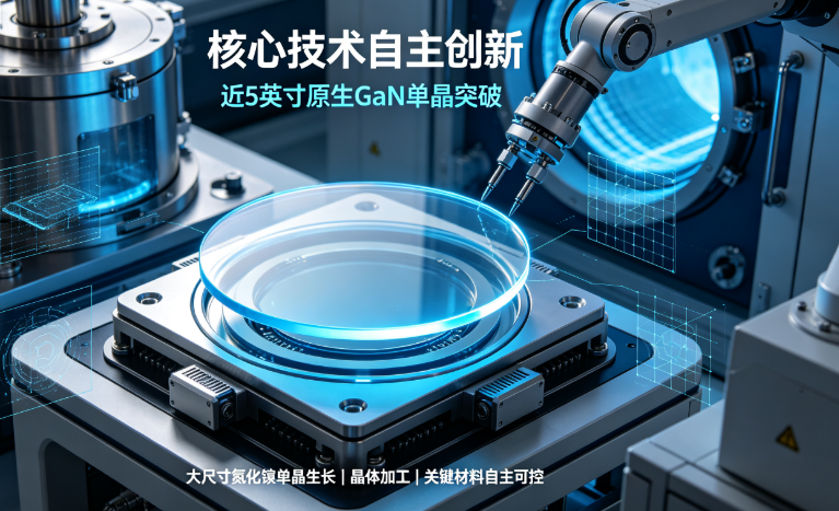
The image above shows the core module of the HVPE growth equipment independently developed by Shandong Jingjia. Through precise heater design and gas flow control, this system achieves consistent crystal quality during multi-wafer growth, laying the foundation for mass production of large-size substrates.
2. Technological Breakthrough: Leap from “Laboratory Sample” to “Production Line Product”
For the industrialization of any cutting-edge technology, the most difficult step is not theoretical breakthrough but the engineering transformation “from sample to product.” Chairman Zhang Lei deeply felt this: “Producing a good crystal in the lab and achieving stable mass production in the factory are two entirely different things—temperature field scaling, airflow field uniformity, yield control—every parameter must be re-explored on an industrial scale, with no shortcuts.”
Shandong Jingjia's solution is to locate the factory area immediately adjacent to the State Key Laboratory of Crystal Materials of Shandong University, forming an ecosystem with zero-distance connection between laboratory and production line. The beauty of this design is that the latest mechanism research results from the lab can be immediately verified on the production line, while engineering problems encountered during mass production on the line can be promptly fed back to the basic research end, forming the shortest iteration loop. This deeply integrated model of “industry, academia, and research” greatly shortens the technology maturity cycle.
At the process level, technological breakthroughs are mainly reflected in three key areas:
First, large-size single-crystal growth. By optimizing the thermal field distribution and gas transport model of the HVPE reaction chamber, the team successfully grew nearly 5-inch native GaN single crystals, setting a domestic record for the largest size. The significance of this size is not just about breaking records; it paves the way for the subsequent development of 6-inch and even 8-inch substrates. In terms of area, a 5-inch substrate increases the effective area of a single wafer by about 6 times compared with a 2-inch substrate, directly affecting the economics of downstream device manufacturing.
Second, low-damage precision processing. GaN crystals have high hardness and brittleness. Traditional grinding and polishing processes tend to cause surface scratches and subsurface damage, affecting substrate quality. Shandong Jingjia independently overcame the full process of low-damage grinding, chemical mechanical polishing (CMP), and cleaning, achieving stable substrate surface roughness below 0.2 nanometers, truly meeting the standard of “open-box ready.” This indicator not only approaches the ultimate level of similar foreign products but also provides a perfect interface for downstream epitaxial growth.
Third, yield and consistency control. By introducing in-line monitoring systems and big data analysis, the team achieved real-time feedback and process parameter adjustment for crystal defects (such as dislocation density and cracks), bringing the mass production yield of 2-inch substrates to an industry-leading level. Currently, Shandong Jingjia has successfully achieved large-scale mass production of 2-inch GaN single-crystal substrates, which are widely used in blue-green lasers, high-end LEDs, microwave communications, and power electronics, significantly reducing the domestic industry's dependence on imported substrates.
3. Industrial Synergy: Unlocking a Key Link in the Semiconductor Industry Chain
GaN single-crystal substrates are at the very top of the semiconductor industry chain, and their quality directly determines the performance of downstream epitaxial wafers, devices, and modules. For a long time, the lack of domestic substrates forced domestic device manufacturers to purchase expensive imported substrates while facing supply disruption risks. Shandong Jingjia's mass production breakthrough brings two major benefits to downstream companies:
First, supply chain security. Chairman Zhang Lei emphasized: “After achieving self-sufficiency, downstream companies no longer worry about supply cutoffs, and can define and develop globally leading devices based on domestic substrates.” This collaborative innovation from the material end to the device end allows domestic companies to optimize substrate parameters according to their own device structures, rather than passively adapting to imported product specifications. For example, in the blue-green laser field, chips based on domestic substrates have achieved photoelectric conversion efficiency comparable to international benchmarks in some leading companies' labs.
Second, cultivation of the industrial ecosystem. As a key enterprise in the semiconductor industry chain nurtured by Jinan City, Shandong Jingjia's demonstration effect is driving the growth of surrounding supporting companies. From specialty gases and graphite parts to inspection equipment, Shandong Province has gradually formed an industrial cluster around third-generation semiconductors. This “point-line-area” diffusion effect is the core logic of Shandong Province's efforts to build new-generation information technology landmark industrial chains.
It is worth mentioning that Shandong Jingjia not only focuses on GaN but also looks toward the more cutting-edge aluminum nitride (AlN) substrates. AlN has a wider bandgap (about 6.2 eV) and higher thermal conductivity (about 320 W/m·K) than GaN, making it an ideal material for next-generation deep ultraviolet optoelectronic devices and high-power RF devices. Zhang Lei announced: “We are committed to promoting the large-scale production of 6-inch large-size substrates while launching AlN substrates as our second product line.” This move demonstrates the company's long-term layout for third-generation semiconductor technology routes.
4. Green Gene: The Internal Logic of GaN Supporting the “Dual Carbon” Goals
GaN inherently possesses a “green gene.” With fast switching speed and low on-resistance, when made into power devices, it can significantly reduce power conversion losses. Taking new energy vehicles as an example, using GaN inverters can increase motor drive efficiency to over 99%, reducing energy consumption by about 50% compared with silicon-based inverters. If this technology is widely applied in the global electric vehicle market, it can save electricity equivalent to hundreds of millions of tons of standard coal each year. Similarly, in photovoltaic energy storage systems, GaN DC-DC converters can improve the power generation efficiency of solar power stations and reduce heat loss during inversion, thereby increasing green electricity utilization.
Chairman Zhang Lei deeply recognizes the company's social responsibility: “Every substrate we produce is a 'basic energy-saving component' supporting the development of energy-efficient industries, directly helping the country achieve its 'dual carbon' goals.” From a life-cycle perspective, although the energy consumption for producing one GaN substrate is higher than that for a same-size silicon substrate, when applied to power electronic devices, the electricity saved throughout its life cycle is tens of times the production energy consumption. This logic of “energy saving from the source” is a key reason why third-generation semiconductors are listed as strategic industries by countries.
Shandong Jingjia's green contribution is not only reflected in the product application side but also in the greening of the production process. In the selection of crystal growth equipment, the company prioritizes low-power heating elements and efficient exhaust gas treatment systems to minimize the carbon footprint of production. In the future, with the scale benefits brought by mass production of large-size substrates, carbon emissions per substrate will further decrease.
5. Future Outlook: The Inevitable Path from Catch-up to Leadership
Looking back at Shandong Jingjia's development history, we can clearly see a trajectory from technological catch-up to partial running alongside, and then to localized leadership. Based on the stable mass production of 2-inch substrates, the company is steadily expanding mature production lines while turning its attention to the large-scale production of 6-inch large-size substrates. According to industry rules, each inch increase in substrate size leads to an exponential increase in usable area per wafer, which is crucial for cost control of downstream devices. Currently, international leading companies have commercialized 6-inch GaN substrates, but yield and uniformity still have room for improvement. If Shandong Jingjia can achieve breakthroughs in this area, it will have the opportunity to occupy a place in global competition.
Of course, challenges remain severe. On one hand, foreign competitors still have significant first-mover advantages in equipment, processes, and patents; on the other hand, there are still shortcomings in supporting links such as high-end inspection equipment and high-purity raw materials in China. But as Zhang Lei said: “There are no shortcuts.” Only by continuously deepening industry-academia-research collaboration and increasing R&D investment can we consolidate existing breakthroughs and advance toward higher goals.
From a broader perspective, the case of Shandong Jingjia is a microcosm of China's independent control of the third-generation semiconductor industry. It proves that under the guidance of national strategy, relying on the basic research accumulation of top universities, combined with the company's engineering capabilities and market insight, it is entirely possible to break foreign monopolies and achieve the leap from “following” to “running alongside” for key materials. As more and more “Shandong Jingjias” emerge, the resilience and competitiveness of China's semiconductor industry chain will surely undergo a qualitative leap.
Conclusion
The localization of GaN single-crystal substrates is not only a breakthrough in a key technology but also an important practice of the national science and technology autonomy strategy in the field of third-generation semiconductors. Relying on continuous innovation in the HVPE route, Shandong Jingjia successfully solved core challenges such as large-size growth, low-damage processing, and mass production yield control, providing reliable key material support for China's strategic emerging industries like 5G communication, new energy vehicles, and high-end displays. At the same time, the significant energy-saving and emission-reduction benefits of its products directly serve the realization of the “dual carbon” goals.
Looking ahead, with the mass production of large-size substrates and the launch of the AlN second product line, Shandong Jingjia is expected to move from “filling gaps” to “global leadership.” This path is full of challenges, but the direction is clear. Only by adhering to independent innovation and bridging the last mile of industry-academia-research cooperation can we truly move from being “choked” to “strengthening the chain,” writing a significant chapter in the independent control of China's semiconductor industry.